|
|
Remote Access
Remote Access Info & Resources
RAIN News and Events
Classroom Resources
Lab guides are formatted in powerpoint for use in the classroom. These are good resources for engaging students and preparing for a remote access session.
- Geology Mineral Lab
- Plant Growth in Solution of Nanoparticles
- Determination of Percent Oxygen in Air
- Gold Nanoparticle Synthesis and Characterization
- Nickel Nanowire Synthesis and Characterization
- Silver Nanowire Synthesis and Characterization
- Dye-Sensitized Nanocrystalline Solar Cell Fabrication and Characterization
- Achoo! Pollen does more than make us sneeze. (NNCI)
- Electroplating: Exploring Factors Effecting Deposition, Morphology, and Thickness of Thin Metallic Layers of Copper. (NNCI)
- Mystery Molecules: Identifying Materials with Nanoscale Characterization Tools (NNCI)
- Seeing Nano I: Using scanning electron microscopy (SEM) to view nano-size objects. (NNCI)
- Seeing Nano II: Using atomic force microscopy to view nano-size objects. (NNCI)
- Silver nanoparticle synthesis, spectroscopy, and bacterial growth. (NNCI)
- Synthesis and Characterization of CdSe Quantum Dots. (NNCI)
- Synthesis and Stability of Silver Nanoparticles. (NNCI)
- Spectrophotemetry of Metal Nanoparticles. (NNCI)
Getting Ready for Remote Access
Watch Videos 
To get the most out of your remote access session, we suggest that teachers and students learn about the technology used to view things at the nano-scale level. Our recommended videos can be viewed in the classroom, or assigned as homework.
Click below to browse videos.
Click below to browse videos.
Complete the Remote Access Request Form
This is where you request a remote test session (if this is your first time running remote access with us) and a live session; select the instruments and
topic areas you’d like to focus on; and provide your lab instructor with other important information such as your class' interests and knowledge level.
See below for information on the instruments available and our partners who are running remote access across the country. Once your request has been received, you will get a confirmation from the Remote Access Manager on your selected dattes, times, and instruments.
See below for information on the instruments available and our partners who are running remote access across the country. Once your request has been received, you will get a confirmation from the Remote Access Manager on your selected dattes, times, and instruments.
Run a remote test session
º This is used to check your audio, video, and Internet connections.
º Takes about 20 minutes.
º Takes about 20 minutes.
Before you start remote access, you’ll need to:
1. Install Video Conferencing Software
º
Based on the instrument and partner site you requested, you will need either Zoom or Team Viewer. Both are free to download and use.
2. Set up your computer. You need:
º Webcam
º Microphone
º Speakers
º A projecter or large display is recommended, but not required
º Microphone
º Speakers
º A projecter or large display is recommended, but not required
Choose your samples
You can use in house samples or send your own to the remote access site you selected when scheduling your session. Based on your remote access request (step 2), a remote access manager will reach out to you regarding in house sample availability and to provide address information for any samples you wish to mail in.
Run a live session
º This is where you will have live remote access to the lab equipment.
º This can take anywhere from 15 minutes to 2 hours.
º This can take anywhere from 15 minutes to 2 hours.
Give us feedback!
Help us show the NSF that remote access is a valuable resource.
Instructor Survey - tell us about your experience requesting, testing, and running remote access.
Student Survey - share this survey with your students. We want to know if they enjoyed the experience and found it valuable.
Instructor Survey - tell us about your experience requesting, testing, and running remote access.
Student Survey - share this survey with your students. We want to know if they enjoyed the experience and found it valuable.
What type of tools are available for remote?
The remote access instrument centers have a wide rarity of microscopes and analytical tools to enable high magnification with high resolution for 2D and 3D imaging and prices measurement of chemical, compositional, or other physical properties, respectfully. Sample libraries at the instrument centers have specimen to cover most interest areas.
For more information on these tools and techniques please reference E SC 216 course notes and training modules.
For more information on these tools and techniques please reference E SC 216 course notes and training modules.
Scanning Electron Microscope (SEM)
A scanning electron microscope (SEM) is a type of electron microscope that produces images of a sample by scanning it with a focused beam of electrons. The electrons interact with atoms in the sample, producing various signals that can be detected and that contain information about the sample's surface topography and composition. The electron beam is generally scanned in a raster scan pattern, and the beam's position is combined with the detected signal to produce an image. SEM can achieve resolution better than 1 nanometer. Specimens can be observed in high vacuum, in low vacuum, in wet conditions (in environmental SEM), and at a wide range of cryogenic or elevated temperatures. Read more
- NCI-SW at Arizona State University - (Phenom Pro)
- CABOCES - (Phenom ProX & JEOL-JSM-6010PLUS/LA)
- Grand Valley State University - (Hitachi S3400N)
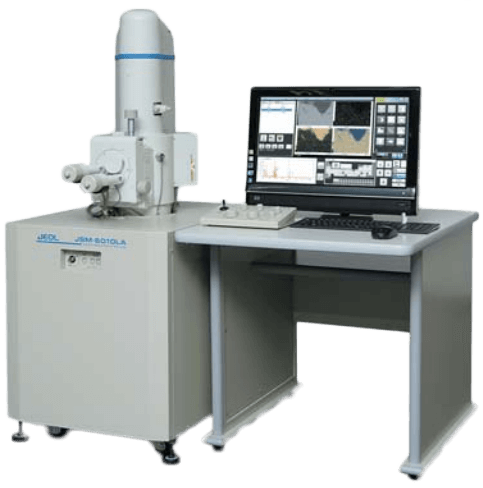
- Erie Community College - (JEOL JSM-6010LA)
- Northcentral Technical College - (Hitachi TM 3030)
- Northwest Vista College - (Hitachi TM 3030 Plus)
- Oakton Community College - (Hitachi TM 3000)
- North Seattle College - (Aspex EXplorer)
- Pasadena City College - (Phenom ProX)
- Pennsylvania State University - (ZEISS 55 Ultra FESEM)
- Research Triangle Nanotechnology Network - (FEI Quanta 200 Field Emission Gun)
- Salt Lake Community College - (Hitachi TM3000)
- SUNY Polytechnic Institute - (Hitachi TM3000 w/ x-ray (EDS))
- University of California San Diego - (Zeiss Sigma 500 SEM)
- University of Texas at San Antonio - (Hitachi S5500 STEM)
- SCME at University of New Mexico - (Phenom ProX)
- Utah Valley University - (TESCAN VEGA3)
Remote Accessibility:
Electron Probe Microanalyzer (EPMA)
What is an Electron Microprobe, how is it different from a Scanning Electron Microscope, and when does a researcher choose the probe vs. the SEM?
An electron microprobe (or electron probe microanalyzer, EPMA) is a specialized scanning electron microscope, optimized for accurate and precise quantitative compositional analysis of solid materials at the micro-scale. In addition to electron imaging capability, it has a reflected light microscope to check focus and surface quality. It is equipped with five wavelength-dispersive X-ray spectrometers (WDS), which use diffracting crystals to separate the characteristic X-rays emiited by a sample before counting them. This gives the EPMA much finer spectral resolution than the energy-dispersive X-ray spectrometers (EDS) often installed on SEMs. In turn, in combination with careful analysis of standards and matrix correction software, WDS allows quantification of all major elements heavier than N and minor elements down in some cases to ~100 ug/g, with typically 1% relative precision and accuracy. Because each WDS spectrometer only counts one wavelength at a time, one usually only analyzes a short list of elements. By comparison, EDS analysis on the SEM achieves only about 5% relative precision and accuracy and generally cannot detect minor elements below ~1000 ug/g, but simultaneously measures all the elements. Hence, when accurate and precise determination of a known list of elements is desired, the EPMA is the instrument of choice. When quicker qualitative assessment of the elements present is desired, the SEM is the tool of choice. EPMA analysis gives a student an opportunity to learn and think about a number of important issues in microanalysis and in the science and statistics of measurement more broadly: choice of standards, background subtraction, counting statistics, reproducibility, detection limits, internal and external precision, etc.
- California Institute of Technology - (JEOL JXA-8200 Hyperprobe, Combined ED/WD Electron Probe Microanalyzer)
Remote Accessibility:
Energy Dispersive Spectroscopy (EDS)
Energy-dispersive X-ray spectroscopy (EDS, EDX, or XEDS), sometimes called energy dispersive X-ray analysis (EDXA) or energy dispersive X-ray microanalysis (EDXMA), is an analytical technique used for the elemental analysis or chemical characterization of a sample. It relies on an interaction of some source of X-ray excitation and a sample. Its characterization capabilities are due in large part to the fundamental principle that each element has a unique atomic structure allowing unique set of peaks on its X-ray emission spectrum. Read more
- Erie Community College - (JEOL JSM-6010LA)
- Grand Valley State University - (EDAX EDS)
- North Seattle College - (Aspex EXplorer)
- Oakton Community College - (Quantax 70)
- Pasadena City College - (Phenom ProX)
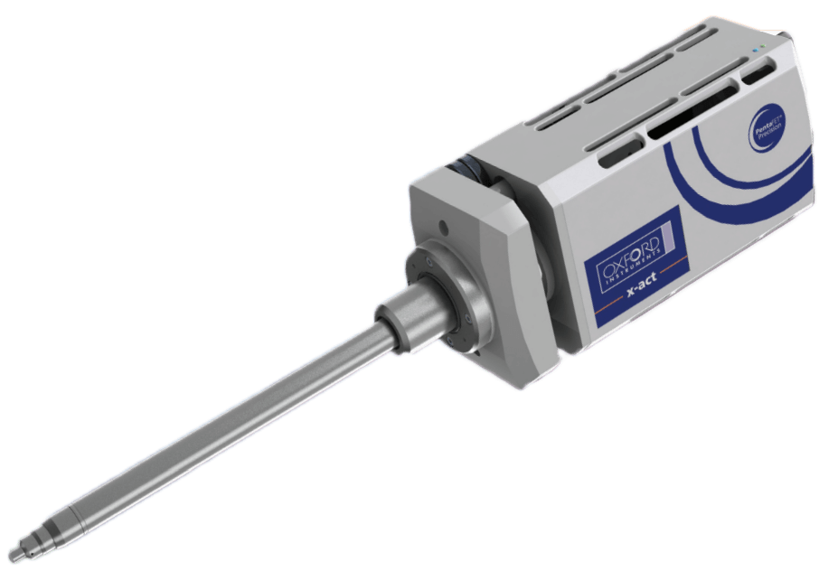
- Pennsylvania State University - (Oxford Instruments X-act)
- University of Texas at San Antonio - (Hitachi S5500 STEM)
Remote Accessibility:
Atomic Force Microscope (AFM)
Atomic-force microscopy (AFM) or scanning-force microscopy (SFM) is a very high-resolution type of scanning probe microscopy (SPM), with demonstrated resolution on the order of fractions of a nanometer, more than 1000 times better than the optical diffraction limit. Read more
- Erie Community College - (AFM)
- Forsyth Tech Community College - (Nanosurf Flex Scan head AFM)
- Georgia Southern University - (Atomic Force Microscopy (AFM) - Park System - NX-10)
- Grand Valley State University - (Agilent 5400 AFM/SPM)
- Northcentral Technical College - (Nanosurf easyScan 2)
- North Seattle College - (Nanosurf easyScan 2)
- Oakton Community College - (Nanosurf easyScan 2 FlexAFM)
- Pennsylvania State University - (Bruker Innova)
- Salt Lake Community College - (Agilent 5400 AFM/SPM & Nanosurf easyScan 2)
Remote Accessibility:
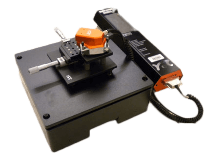
Profilometer
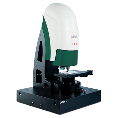
Profilometer is a measuring instrument used to measure a surface's profile, in order to quantify its roughness. Read more
- North Seattle College - (Bruker Dektak XT)
- Oakton Community College - (Bruker Dektak XT)
- Pennsylvania State University - (Veeco Dektak 6M)
Remote Accessibility:
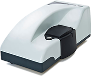
Ultraviolet–visible Spectrophotometer
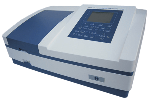
Ultraviolet–visible spectroscopy or ultraviolet-visible spectrophotometry (UV-Vis or UV/Vis) refers to absorption spectroscopy or reflectance spectroscopy in the ultraviolet-visible spectral region. This means it uses light in the visible and adjacent (near-UV and near-infrared [NIR]) ranges. The absorption or reflectance in the visible range directly affects the perceived color of the chemicals involved. Read more
- Coppin State - (UV-VIS-NIR Spectrophotometer)
- Georgia Institute of Technology - (Thermo UV-VIS Spectrometer)
- Pennsylvania State University - (Cary 300)
Remote Accessibility:
Confocal Microscope
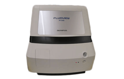
Confocal microscopy is an optical imaging technique for increasing optical resolution and contrast of a micrograph by means of adding a spatial pinhole placed at the confocal plane of the lens to eliminate out-of-focus light. It enables the reconstruction of three-dimensional structures from the obtained images. Read more
- Stanford University - (Keyence 3D Laser Confocal Scanning Microscope)
- North Seattle College - (Olympus Fluoview FV10i)
Remote Accessibility:
Optical Microscope
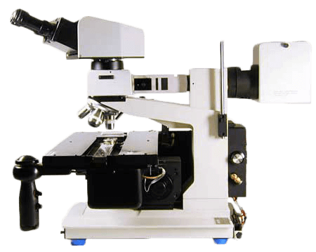
The optical microscope, often referred to as light microscope, is a type of microscope which uses visible light and a system of lenses to magnify images of small samples. Optical microscopes are the oldest design of microscope and were possibly invented in their present compound form in the 17th century. Basic optical microscopes can be very simple, although there are many complex designs which aim to improve resolution and sample contrast. Read more
- Pennsylvania State University - (Leitz Ergolux)
Remote Accessibility:
Molecular Analyzer
The molecular analyzer is used for the measurement of the size, electrophoretic mobility of proteins, zeta potential of colloids and nanoparticles, and optionally the measurement of protein mobility and microrheology of protein and polymer solutions.
- Georgia Institute of Technology - (Malvern Zetasizer Nano ZS)
Remote Accessibility:
Fourier Transform Infrared Spectroscopy (FTIR)
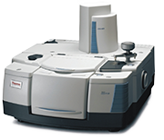
Fourier transform infrared spectroscopy (FTIR) is a technique which is used to obtain an infrared spectrum of absorption or emission of a solid, liquid or gas. An FTIR spectrometer simultaneously collects high spectral resolution data over a wide spectral range. This confers a significant advantage over a dispersive spectrometer which measures intensity over a narrow range of wavelengths at a time. Read more
- Georgia Institute of Technology - (Thermo Scientific iS50 FT-IR Spectrometer)
Remote Accessibility:
X-ray fluorescence (XRF)
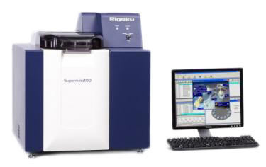
X-ray fluorescence (XRF) is the emission of characteristic "secondary" (or fluorescent) X-rays from a material that has been excited by bombarding with high-energy X-rays or gamma rays. The phenomenon is widely used for elemental analysis and chemical analysis, particularly in the investigation of metals, glass, ceramics and building materials, and for research in geochemistry, forensic science, archaeology and art objects such as paintings and murals. Read more
- Nebraska Nanoscale Facility - (Rigaku Supermini200 X)
Remote Accessibility:
Fabrication Tools
The following fabrication tools are available:
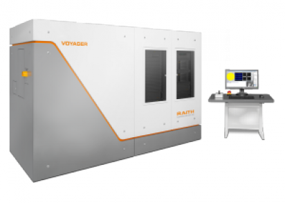
Raith Voyager Electron Beam Lithography tool
Electron Beam Deposition, Angstrom Engineering, Model 450
Reactive Ion Etching tool, NGP80, Oxford Instruments
Reactive Ion Etching tool, TRION (Norfolk State University)
FIB FEI Nova 600 Nanolab (Dual Beam) with FESEM capability (COSINC)
- University of Iowa
- Norfolk State University
- COSINC at University of Colorado Boulder
Remote Accessibility:
Rough Vacuum Equipment Trainer (RA-RVET)
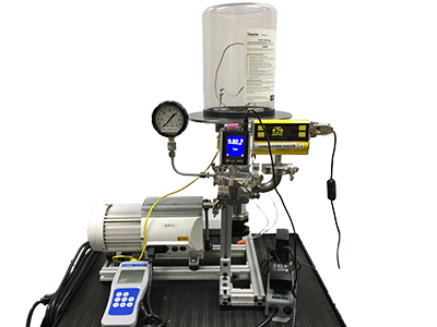
- Normandale Community College - (Custom Built Training System (RA-RVET))
Remote Accessibility:
Remote Instrument Partners Who we are
Remote access instrument centers are located across the continental US so we may serve the widest possible community–anyone who wants to learn about nanotechnology. Each center has tools of unique functionality, all with micro and nano capabilities.
The centers are staffed by a number of people with special education and research interests, but all have a strong foundation in nanotechnology in their related fields as well as practical experience with microscopes and analytical instrumentation. Our remote instrument managers are all dedicated to the improvement of science and engineering education and to helping their communities flourish.
We thank them for their time and dedication.
Partners
Arizona State University (NCI-SW at ASU)
Cattaraugus-Allegany-Erie-Wyoming Board of Cooperative Educational Services (CABOCES)
California Institute of Technology
Colorado Shared Instrumentation in Nanofabrication and Characterization (COSINC)
Coppin State
Erie Community College (ECC)
Forsyth Tech Community College
Georgia Institute of Technology
Georgia Southern University
Grand Valley State University
Nebraska Nanoscale Facility
Norfolk State University (SCENE)
Northcentral Technical College (NTC)
Normandale Community College
Northwest Vista College, Workforce Programs
North Seattle College (NSC - SHINE)
Oakton Community College (O.R.A.N.G.E.)
Pasadena City College (PCC)
Pennsylvania State University (CNEU - NACK Network)
Research Triangle Nanotechnology Network (RTNN)
Salt Lake Community College (SLCC)
Stanford University (nano@Stanford)
SUNY Polytechnic Institute
University of Iowa
University of California San Diego
University of Texas at San Antonio (UTSA)
University of New Mexico (SCME)
Utah Valley University (UVU)
Normandale Community College
Normandale Community College
Bloomington, MN
Contact:
Chair, Engineering Technology ProgramsNancy Louwagie
Nancy.Louwagie@normandale.edu
952-358-8738
Tool(s):
- Remotely Accessible Rough Vacuum Equipment Trainer system (RA-RVET)
COSINC (Colorado Shared Instrumentation in Nanofabrication and Characterization)
University of Colorado Boulder
Boulder, CO
Contact:
COSINC-CHR Facility Manager/ScientistTomoko Borsa
borsa@colorado.edu
303-735-0203
COSINC Director
Aju Jugessur
Aju.Jugessur@colorado.edu
303-735-5019
Grand Valley State University
Grand Rapids, MI
Contact:
Program Chair of Electrical EngineeringDr. Heidi Jiao, Professor of Electrical Engineering
Jiaoh@gvsu.edu
616-331-6844
California Institute of Technology
California Institute of Technology
Pasadena, CA
Contact:
Instrument OperatorChi Ma
chima@caltech.edu
626-395-6126
Principal Investigator
Paul Asimow
asimow@caltech.edu
626-395-4133
Tool(s):
- JEOL JXA-8200 Hyperprobe, Combined ED/WD Electron Probe Microanalyzer
The Nanotechnology Collaborative Infrastructure Southwest (NCI-SW) at Arizona State University (ASU)
Arizona State University (ASU)
Tempe, AZ
Cattaraugus-Allegany-Erie-Wyoming Board of Cooperative Educational Services (CABOCES)
Olean and Ellicottville, NY
Contact:
CTE Administrator for Curriculum and InstructionJames Schifley
James_Schifley@CABOCES.org
716-376-8348
Coppin State
Baltimore, MD
Erie Community College (ECC)
Williamsville, NY
Forsyth Tech Community College
WInston-Salem, NC
Georgia Institute of Technology
Atlanta, GA
Contact:
Nebraska Nanoscale Facility
855 N 16th St, N214 NANO
Lincoln, NE 68588-0298
Lincoln, NE 68588-0298
Contact:
Research TechnologistDr. Anandakumar Sarella
asarella@unl.edu
402-472-6087
Materials and Nanoscience Research Specialist II
Dr. Shah Valloppilly
shah@unl.edu
402-472-3693
Georgia Southern University
Georgia Southern University
Statesboro, Georgia
Norfolk State University (SCENE)
Norfolk, Virginia
Northcentral Technical College (NTC)
Northcentral Technical College (NTC)
Wausau, WI
Northwest Vista College, Workforce Programs
Northwest Vista College
San Antonio, TX
Contact:
Stanford University
Stanford, CA
Contact:
Academic program managerAngela Hwang
aahwang@stanford.edu
650-207-8806
External user coordinator
Graham Ewing
grahamj.ewing@stanford.edu
650-498-5653
North Seattle College (NSC)
Seattle, WA
Contact:
O.R.A.N.G.E. (Oakton Remote Access to Nanotechnology Guidance for Educators)
Oakton Community College (O.R.A.N.G.E.)
Skokie, IL
Pasadena City College (PCC)
Pasadena City College (PCC)
Pasadena, CA
Pennsylvania State University (PSU)
State College, PA
Tool(s):
- FESEM: Zeiss 55 Ultra with Oxford Inca EDS
- SPM/AFM: Innova
- Profilometer
- UV-Vis. Spectrophotometry
- EDS
- Optical
Research Triangle Nanotechnology Network (RTNN)
Raleigh, NC
Salt Lake Community College (SLCC)
Salt Lake Community College (SLCC)
Salt Lake City, UT
Contact:
Glen Johnsonglen.johnson@slcc.edu
801-957-4160
Wesley Sanders
Wesley.Sanders@slcc.edu
801-957-3894
SUNY Polytechnic Institute
SUNY Polytechnic Institute
CESTM L241
251 Fuller Rd
Albany, NY 12203
251 Fuller Rd
Albany, NY 12203
University of Texas at San Antonio (UTSA)
One UTSA Circle
San Antonio, TX
San Antonio, TX
Contact:
.
University of Iowa
Iowa City, IA
Contact:
Tool(s):
- Electron Beam Lithography
- Electron Beam Deposition
- Reactive Ion Etching Tool
University of California San Diego
San Diego, CA
Contact:
Director, Education Programs and OutreachYves Theriault, PhD, PMP
ytheriault@ucsd.edu
858-210-0543
Utah Valley University (UVU)
Utah Valley University (UVU)
800 West University Parkway
Orem, UT 84058
Orem, UT 84058
Contact:
Associate ProfessorDr. Paul Weber
Paul.Weber@uvu.edu
801-863-8692
Daniel Rodriguez
danielrdrgz24@gmail.com
385-223-9891
University of New Mexico (SCME)
800 Bradbury Dr. SE
Albuquerque, NM 87106
Albuquerque, NM 87106
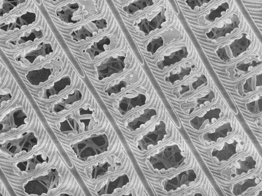
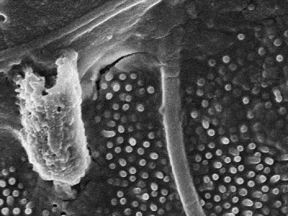
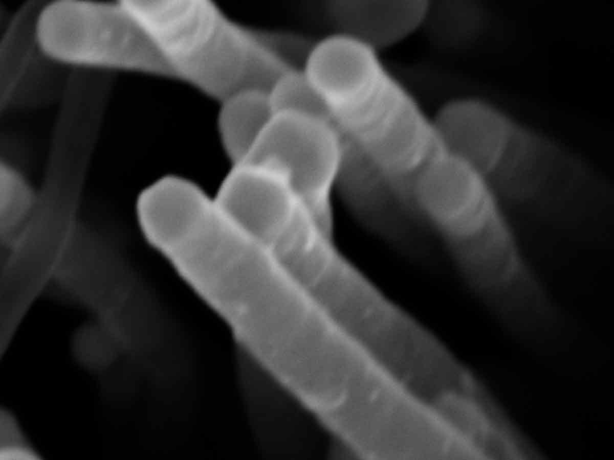
Gallery
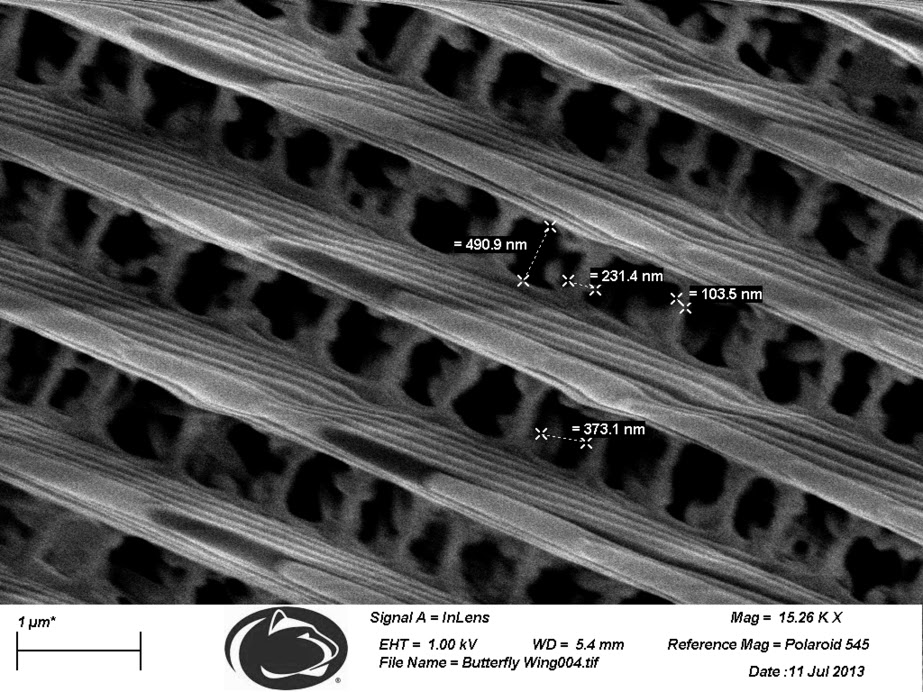
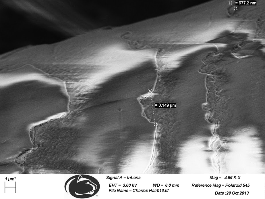


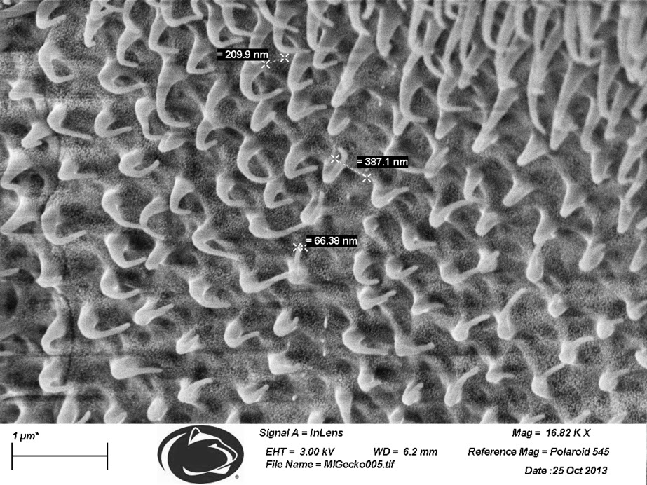

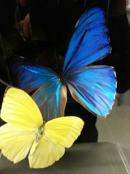
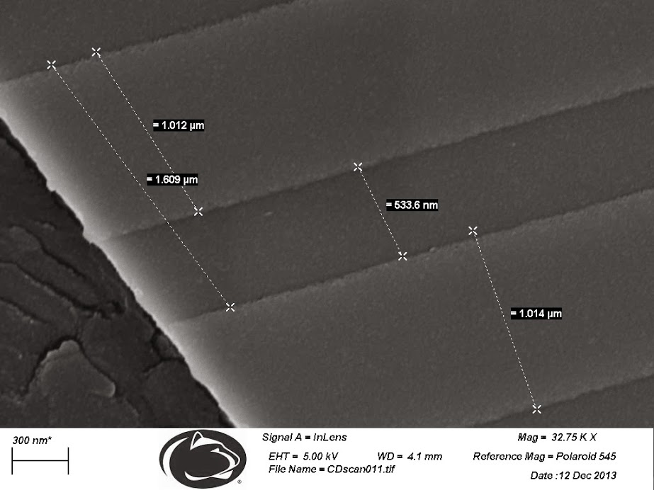
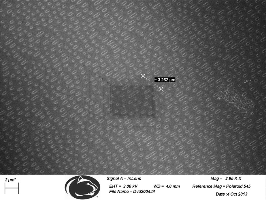

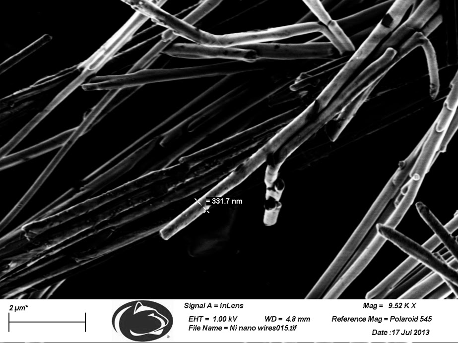
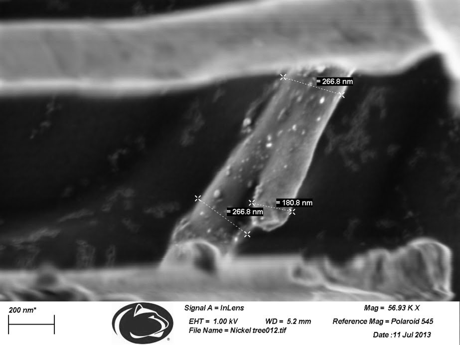
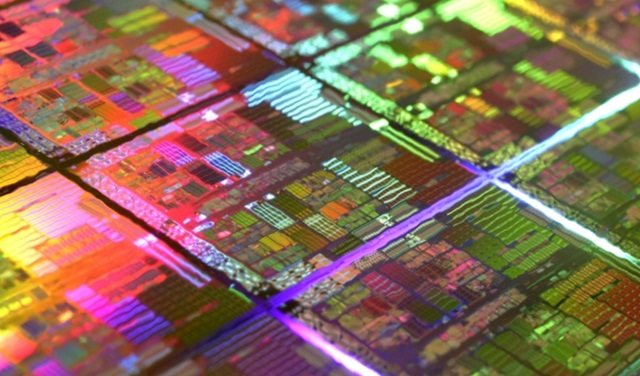
The above nano-scale images are captured with the same tools available for your use (for education or outreach) via our remote access service. Each RAIN partner has samples available, which vary by location. If you have any specific items that you'd like to view during your session, let us know when requesting your session and we will provide you with shipping instructions.

Funded, in part,
by a grant from
the National Science
Foundation.
DUE 2000725
DUE 2000725
