Stephen J. Fonash
Spanish Nano Glossary
A
Actin
A
contractile protein found in muscle cells. Together with myosin, actin provides the mechanism for muscle contraction.
Adsorbate
A substance that becomes
adsorbed at the interface or into the interfacial layer of another
material, or adsorbent.
Albumin
The main protein in human
blood and the key to the regulation of the osmotic pressure of blood.
Chemically, albumin is soluble in water, precipitated by acid, and
coagulated by heat.
Allowed
energies
When electrons are trapped in structures such as in an atom or in a quantum dot, they are allowed by
nature to
have only certain energies. These are called allowed energies. The F=ma
physics approach does not predict this fact of nature but the quantum
mechanics approach does.
Anisotropic
Not
isotropic. Physics. Having properties that differ according to the
direction of measurement.
Anneal
To subject (glass or metal)
to a process of heating and slow cooling in order to toughen and reduce
brittleness.
Antibodies
Specialized proteins
produced by the cells of the immune system that counteract a specific
foreign substance. The production of antibodies is the first line of
defense in the body’s immune response.
Antigens
(Also known as immunogens.)
Substances that can stimulate an immune response. Antigens are usually
proteins or polysaccharides and include the coats, capsules, cell
walls, flagella, fimbrae, and toxins of parasites, bacteria, viruses,
and other microorganisms.
Assembly
A set of pieces that work
together in unison as a mechanism or device.
Atomic
force
microscope
A
scientific instrument which uses the deflection of a nanoscale tip at
the end of a cantilever to image a surface. The deflection at each
given point on a surface of an object is processed by a computer to
create an image of the surface which then can be observed by the human
eye. Because the tip is so small and the deflection detection used is
so precise, the atomic force microscope (AFM) only responds to a
nano-sized region of the surface giving a very detailed
computer-generated picture of the surface.
Atoms
The basic
building blocks of matter. A chemical compound (i.e., a molecule) is
made of atoms arranged in a fixed relationship and according to a fixed
recipe. Every solid, liquid, and gas is made of atoms. There are about
92 different types of naturally occurring, stable atoms. These
different types are referred to as the elements. There are some
man-made atoms but these are made in accelerators and are not stable.
They only exist for a fraction of a second. Atoms are electrically
neutral; i.e., they have no net electrical charge.
ATP
Adenosine triphosphate, a
high energy phosphate compound found in the body; one of the major
forms of energy available for immediate use in the body.
Auger
Electron
Electrons emitted during
radiationless inner shell ionization of an atom.
up
B
Bacteria
A bacterium is a microorganism life form made up of one cell with no
cell nucleus. The plural is bacteria.
Backscattered
Electrons
Produced by an incident
electron colliding with the nucleus of an atom in the specimen. The
incident electron is then scattered backward about 180 degrees with no
appreciable loss of energy, an elastic collision.
Bands
of Allowed Energies
When atoms are brought
together to form a material, the available energy levels adjust to
accommodate the neighboring atoms. The energy levels tend to adjust
into separated groups of energy levels called "energy bands." This is
not inherently a spacial separation; rather it is a difference in the
energy values which are available to the electrons.
Basic
Materials
Essential, fundamental
substances used as inputs to production or manufacturing.
Biological
Assembly
A group of living things that fit together to form a self-contained
unit.
Bleach
To make white or colorless
by means of chemicals or the sun's rays.
Bottom-Up
nanofabricaton
In nanotechnology, the
construction of machines by arranging atoms and molecules into more
complex assemblies.
Brownian
Motion
Motion of a particle in a
fluid owing to thermal agitation,
Buckeyball
Short for
buckminsterfullerene - molecules made up of 60 carbon atoms arranged in
a series of interlocking hexagonal shapes, similar to a soccer ball.
Building
Blocks
Units of
construction or composition.
up
C
Carbon
Nanotube
A cylinder-shaped structure
resembling a rolled-up sheet of graphite that can be a conductor or
semiconductor depending on the alignment of its carbon atoms.
Catalyst
A substance
that increases the rate of a chemical reaction, without being consumed
or produced by the reaction.
Cell
The basic unit of life of which all living matter is constituted.
Channel
The region under the gate through which current flows from the source
to the drain contacts, when the transistor is turned on.
Chemical
Assembly
Process in which a
disordered system of pre-existing components forms an organized
structure or pattern as a consequence of specific, local interactions
among the components themselves, without external direction.
Chemical
Bonding
When atoms are held together in
a
precise relationship due to the interactions of their outer electrons.
Chemical
Etching
Etching process where the
removal of material is due to chemical reactions with the substrate.
Chemical
Properties
A description of the way in
which a substance reacts with another substance to change its
composition.
Chemical
Reaction
A process in which one
substance is transformed into another.
Chemical
Vapor
Growth (Deposition)
This high temperature
coating process, as it relates to tooling applications, involves the
deposition of a solid material onto a heated substrate via a chemical
reaction from a gas phase. This process can be done in atmosphere or
vacuum.
Chip
A piece of semiconductor containing many electronic devices. A chip
will usually contain the transistors and circuits needed for some
function such as a memory chip. Today a chip can contain as many as a
billion transistors.
Colloidal
Chemistry
The subject of interface
and colloid science.
Colloidal
Solutions
A type of mechanical
mixture where one substance is dispersed evenly throughout another.
Because of this dispersal, some colloids have the appearance of
solutions. A colloidal system consists of two separate phases: a
dispersed phase (or internal phase) and a continuous phase (or
dispersion medium). A colloidal system may be solid, liquid, or gaseous.
Complimentary
DNA
Single-stranded
DNA
made in the laboratory from a messenger RNA template under the
aegis of the enzyme reverse transcriptase. This form of DNA is often
used as a probe in the physical mapping of a chromosome. Abbreviated as
cDNA.
Composition
A mixture of ingredients.
Computer
Data
File
A file maintained in
computer-readable form.
Contact
A region designed to allow electric current flow into or out of an
electronic device. Synonymous with terminal and electrode.
up
D
Dark
Field
An illumination technique that makes the sample appear luminous against
a background of little or no light.
Dendrimer
Artificial molecule
structure that has tiny branches or sprigs sprouting from it, which
allow it to carry drug molecules.
Deposition
Deposition is a process in
which gas transforms into solid (also known as desublimation). The
reverse of deposition is sublimation.
Diamond-like
bond
A carbon chemical bonding
configuration in which each carbon atom shares one electron with each
of four adjacent carbon atoms. This is the chemical bonding found for
carbon in diamonds.
Dip
Pen Lithography
(DPN) is a
scanning probe lithography technique where an atomic force microscope
tip is used to transfer molecules to a surface via a solvent meniscus.
DNA
Strains
A section of DNA that
differs in trivial ways from similar groups.
Drain
The heavily doped region in
semiconductor substrates located at the end of the channel in Field
Effect Transistors; carriers are flowing out of the transistor through
the drain.
Drug Molecules
Substances used in medicine to treat diseases or conditions.
Dry
Chemical/Physical Etching
Also called Reacitve Ion
Etching (RIE), A directed chemical etching process used in micro/nano
fabrication in which chemically active ions are accelerated along
electric field lines to meet a substrate perpendicular to its surface.
Dry
Physical Etching
Also called Sputter
Etching, bombardment of the target (substrate) by high energy ions
(e.g. Ar+) extracted from plasma for the purpose of material removal
from the target (etching); highly anisotropic, highly non-selective
etching method.
up
E
E-beam
Lithography
Using
electron beams to create the mask patterns directly on a substrate. The
wavelength of an electron beam is only a few picometers compared to the
248 to 365 nanometer wavelengths of light used to create the
traditional photomasks.
Electrical
Properties
Properties of a substance
which determine its response to an electric field, such as its
dielectric constant or conductivity.
Electrode
A region designed to allow electric current flow into or out of an
electronic device. Synonymous with terminal and contact.
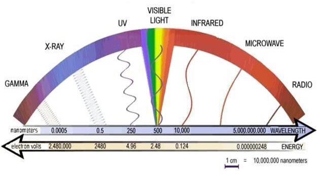
Electomagnetic
spectrum
Energy composed of electric field and magnetic filed components which
propagates as a wave at the speed of light. Radio waves, visible light,
microwaves, x-rays, and infra-red are some of the wavelength (or
equivalently energy) ranges in the electromagnetic spectrum. The full
spectrum is seen in the figure below which gives wavelengths and the
corresponding energy.
Electron
Negative particles that surround the nucleus of the atom. They have
mass, charge, and magnetic moment.
Electron
microscope
A scientific instrument that employs a beam of electrons, generated
just as they are in a conventional (CRT) television tube, which passes
through or bounces back off of an object,. The amount of the beam that
passes through or bounces back is used to image and magnify the objects
by manipulating the electrons using electric and magnetic fields. The
microscope that uses electrons passing through the object for imaging
is termed a transmission electron microscope. (TEM). The microscope
that uses electrons bouncing back from the object for imaging is termed
a scanning electron microscope (SEM). In both the TEM and the SEM, the
electron beam intensities coming through or bouncing back from the
object are processed by a computer to create an image that then can be
observed by the human eye.
Element
A type of atom. There are only
92
naturally occurring types of atoms; i.e., there are only 92 elements.
Embossing
Lithography
A technique for the
fabrication of nanostructures on large surfaces. The method is based on
the excellent replication fidelity obtained with polymers and combines
thermo-plastic molding with common pattern transfer methods.
Emitted
Light
Light coming from an atom, quantum dot, or any material.
Environment
The local physical and chemical situation around a body. (A slightly
different meaning than the everyday usage referring to the air, water,
etc quality experienced by an individual.)
Etch
Rate
The speed at which etching
occurs. Typically measured in Angstroms per second.
Etching
The removal of selected
portions of a layer of material from a substrate using a chemical or
electrolytic process.
Excited
state
Occurs when some of the electrons trapped in a system such as an atom
or quantum dot have acquired enough energy to move up in energy to
normally empty higher allowed
energies.
External
Pattern
Control
Creation of a pattern
through the use of various types of materials, light, heat, and a
predesigned pattern.
Externally
Imposed
Patern
A pattern applied to a
substrate through the use of external pattern control techniques such
as photolithography.
up
F
Fabrication
The act of constructing
something (as a piece of machinery).
Field
Effect
Transistor (FET)
In these devices, the control contact is called the gate. The gate,
which literally gates (allows or disallows) current, uses the voltage
applied to it to create a channel underneath it. The other two contacts
into which and out of which current easily flows are termed the source and drain. Current
from the source to the drain is enabled when the gate is turned on to
create the channel. These devices are often referred to as FETs.
Field
Emission
Electron Microscope
A form of TEM or SEM which employs a beam of electrons produced by quantum mechanical tunneling. In microscopy, this
tunneling process has been traditionally called field emission (FE).
The TEM version is referred to as a FETEM. The SEM version is referred
to as a FESEM. Such instruments are capable of “seeing” very small
objects (including atoms in the case of the FETEM). In both the FETEM
and the FESEM, the electron beam intensities coming through or bouncing
back from the object are processed by a computer to create an image
that then can be observed by the human eye.
Field
Emission Scanning Electron Microscope
A field
emission microscope where the electron beam scans the sample and the
electron information used to create the image originates from either
the origional electron beam which has been deflected off the sample
surface into a detector (backscatter emission), or from the sample's
surface electrons which have been ejected due to the impact of the
electron beam (secondary emission).
Field
Emission Transmission Electron Microscope
A field emission microscope where the electron beam scans the sample
and the electron information used to create the image originate from
the origional electron beam which has been modified after passing
through the sample.
Flagellar
Micromotor
A microscale motor made of
Flagellum; fine hair like structures on cell walls used for locomotion.
Flash
Lithography
An imprint lithography
method utilizing a low viscosity, photo-curable liquid, and a
transparent, rigid template.
Fluoresce
Produce
light when exposed to radiation of a particular wavelength.
Fluorescence
Light emitted when electrons in excited
state energies in an atom, molecule, quantum dot, or material give
up energy by falling back to their ground
state.
Fluorophores
Molecular label conjugated
to an antibody that emits fluorescent light within a measurable color
spectrum in response to a specific wavelength of laser light or
chemical interaction.
Forbidden
Energies
Electrons trapped in a very small structure such as in an atom or in a
quantum dot, they are allowed by nature to have only certain energies.
The energies that are not permitted constitute the forbidden energies.
Friction
The resistance encountered
when one body is moved in contact with another.
Fuel
Cells
A device that converts the
energy of a fuel directly to electricity and heat, without combustion.
Functionalized
Chemically changed with the addition of molecules which are attached by
chemical bonding. These molecules, in turn, can be used to bond to
other substances.
up
G
Gate
An electrode in field effect
transistors (FETs) which has a bias applied to it to induce or turn
off a current flowing between the other two electrodes (i.e., between
the source and drain). Almost negligible current flows into or out of
the gate electrode.
Graphite-Type
Bond
A carbon chemical bonding
configuration in which each carbon atom shares one electron with each
of three adjacent carbon atoms. A fourth electron spends half the time
above and half the time below each carbon atom. This is the chemical
bonding found for carbon in graphite.
Ground
State
Occurs when all the electrons trapped in a system such as an atom or
quantum dot occupy the lowest allowed
energies.
up
H
Hybrid
Anything that is a mixture
of two different things.
Hybrid
Nanofabrication
Nanofabrication utilizing
both top-down and bottom-up nanofabrication tools and techinquies.
Hybrid
Structures
Structures
created by hybrid nanofabrication techniques.
Hydrophobic
Repelling,
tending not to combine with, or incapable of dissolving in water.
Hydrophobicity
The Property of being
hydrophobic.
up
I
Infra-red
That part of the electromagnetic
spectrum which has energies just below that of the visible part of
the spectrum. Equivalently, it has wavelengths just above that of the
visible part of the spectrum.
Inherent
Pattern
The pattern
created naturally by a material.
Ion
An atom or molecule (compound) which has lost or gained one or more
electrons. It is, therefore, electrically charged.
Ion
Beam Lithography
A variation of the electron
beam lithography technique, using a focused ion beam (FIB) instead of
an electron beam. In a similar setup to scanning electon microscopes,
an ion beam scans across the substrate surface and exposes electron
sensitive coating.
Ion
Channels
A protein-coated pore in a
cell membrane that selectively regulates the diffusion of ions into and
out of the cell.
Ionized
The state in which an atom
is missing one or more of its electrons, and is therefore positively
charged.
Isotropic
In a subtractive process,
the material is removed in all directions simultaneously, frequently at
the same rate vertically and horizontally.
up
J
up
K
Kinesin
A family of microtubule
motor proteins active in mitosis. The kinesins use chemical energy from
the hydrolysis of ATP (adenosine triphosphatase) to generate mechanical
force. They bind tightly to and move along the microtubules.
up
L
Layers
A single thickness, coat,
fold, or stratum.
Linear
Micromotors
A micro-scale linear motor.
A linear motor is a multi-phase alternating current (AC) electric motor
that has had its stator "unrolled" so that instead of producing a
torque (rotation) it produces a linear force along its length.
Lithography
The process of copying a
pattern onto a surface using light, electron beams, or X-rays.
Living
Tissues
Any tissue of a living
organism containing cells that are being replaced when they die.
Lymph
Node
Gland that makes up part of
the immune system that removes bacteria and foreign particles from the
body.
Lymph
System
The tissues and organs that
produce, store, and carry white blood cells that fight infection and
other diseases. This system includes the bone marrow, spleen, thymus
and lymph glandsand a network of thin tubes that carry lymph and white
blood cells into all the tissues of the body.
up
M
Macromolecule
A very large molecule, such
as a polymer or protein, consisting of many smaller structural units
linked together. Also called supermolecule.
Manufacturable
If something is manufacturable or possess manufacturability, it can be
made reliably and economically.
Mask
The pattern used in
lithography that determines which areas are exposed and which are not.
Material
Modification
The act of making changes
in form or character to a material.
Mechanical
Processes
The branch of physics
concerned with the behaviour of physical bodies when subjected to
forces or displacements, and the subsequent effect of the bodies on
their environment.
Mechanical
Properties
The properties of a
material that reveal its elastic and inelastic (plastic) behavior when
force is applied, thereby indicating its suitability for mechanical
(load-bearing) application, fatigue limit, hardness, modulus of
elasticity, tensile strength, and yield strength.
Meter
A basic unit of length used in the metric system. In terms of the
English set of length units, one meter is 39.4 inches or equivalently
3.28 feet in length.
Microscopy
The examination of minute
objects by means of a microscope, an instrument which provides an
enlarged image of an object not visible with the naked eye.
Microtubules
A minute filament in living
cells that is composed of the protein tubulin and occurs singly, in
pairs, triplets or bundles. Microtubules help cells to maintain their
shape; they also occur in cilia, flagella and the centrioles, and form
the spindle during nuclear division.
Modification
Alteration: the act of
making something different.
Mold
A frame or model around or
on which something is formed or shaped.
Molecule
Synthesis
The
formation of molecules from simpler compounds or elements.
Molecules
The smallest division of a
compound that still retains or exhibits all the properties of the
substance.
Moltronics
Also called molecular
electronics, an interdisciplinary theme that spans physics, chemistry,
and materials science. The unifying feature of this area is the use of
molecular building blocks for the fabrication of electronic components,
both passive (e.g. resistive wires) and active (e.g. transistors).
Monolayer
A monolayer is a single, closely packed layer of atoms, molecules, or
cells.
up
N
Nano-Electronics
Investigation, fabrication,
characterization and application of functional electron devices with
dimensions below 100 nm.
Nanofabrication
Fabrication, such as
building or sculpting, at the nanoscale, on the level of individual
molecules.
Nano-Imprinting
A method of fabricating
nanometer scale patterns. It is a simple process with low cost, high
throughput and high resolution. It creates patterns by mechanical
deformation of imprint resist and subsequent processes. The imprint
resist is typically a monomer or polymer formulation that is cured by
heat or UV light during the imprinting. Adhesion between the resist and
the template is controlled to allow proper release.
Nano-Indentation
Depth-sensing indentation
testing in the submicrometer range and has been made possible by the
development of 1) machines that can make such tiny indentations while
recording load and displacement with very high accuracy and precision,
and 2) analysis models by which the load displacement data can be
interpreted to obtain hardness, modulus, and other mechanical
properties.
Nanoparticle
Any microscopic particle
less than about 100 nanometers (nm) in diameter.
Nanostructure
An arrangement, structure, or part of something of molecular dimensions.
Nanotube
A nanoscale tube-like structure, which can occur naturally in some
minerals, or be man-made from a variety of materials including carbon.
Nanowire
A wire of a
material (for example, a metal), the diameter of which is less than 100
nm.
Near-Infra-Red
That part of the infra-red range of the electromagnetic
spectrum which is closest in energy (or, equivalently wavelenght)
to red.
Non-Destructive
Testing
Generic term for all
material tests, which detect material irregularities without damaging
the work-piece.
Non-Invasive
Testing or measurement of some sample that is done without disturbing
the sample.
up
O
On-State
An operating condition of a
transistor whereby the voltage and resistance between the source and
drain are such that electron flow between them is possible.
Optical
Lithography
A process used to
selectively remove parts of a thin film (or the bulk of a substrate).
It uses light to transfer a geometric pattern from a photomask to a
light-sensitive chemical (photoresist, or simply "resist") on the
substrate. A series of chemical treatments then engraves the exposure
pattern into the material underneath the photoresist.
Optical
Microscope
A scientific instrument that employs light manipulated using lenses to
magnify objects. The image produced can be observed directly by the
human eye without computer processing.
up
P
Particle
A body
having finite mass and internal structure but negligible dimensions.
Pathological
Pertaining to pathology,
the path of medicine that treats the essential nature of disease.
Photo
Lithography
Also called optical
lithography, it is a process used to selectively remove parts of a thin
film (or the bulk of a substrate). It uses light to transfer a
geometric pattern from a photomask to a light-sensitive chemical
(photoresist, or simply "resist") on the substrate. A series of
chemical treatments then engraves the exposure pattern into the
material underneath the photoresist.
Photon
The quantum of
electromagnetic energy, regarded as a discrete particle having zero
mass, no electric charge, and an indefinitely long lifetime.
Physical
Application
To put on a surface through
physical means.
Physical
Assembly
To assemble through
physical means.
Physical
Contact
The act of
touching physically, so that no air gaps exist between the materials.
Physical
Fabrication
To fabricate through
physical means.
Physical
Properties
A description of the
qualities of a substance that can be demonstrated without changing the
composition of the substance.
Physical
Vapor
Deposition
Also termed “atomic
deposition” is a process in which material vaporized from a source is
transported in the form of a vapor through a vacuum to the substrate
where it condenses.
Physiological
Of, or relating to physiology;the study of the mechanical, physical,
and biochemical functions of living organisms.
Planar
Structure
Structures
having a two-dimensional characteristics.
Plasma
A low-density gas in which individual atoms are ionized.
Polymer
A high molecular weight organic compound, natural or synthetic, whose
structure can be represented by a repeated small unit, the monomer (eg,
polyethylene, rubber, cellulose).
Positive
Ion
An atom having a net positive charge due to the loss of one of its
negatively charged electrons.
Probe
An object or device used to investigate the unknown.
Protein
Complex organic molecules made up of amino acids. These molecules a key
to cell functioning.
Proton
One of the basic particles
which makes up an atom. The proton is found in the nucleus and has a
positive electrical charge equivalent to the negative charge of an
electron and a mass similar to that of a neutron.
up
Q
Quantum
dot
A nano-scale arrangement of atoms in a ball shape usually from about
2nm to 50nm in diameter. The atoms used are ones which form
semiconductors or insulators since these structures are used for their
optical and electrical properties. Quantum effects often dominate in
these very small structures giving them their name.
Quantum
Mechanical
Of or
pertaining to Quantum Mechanics.
Quantum
Mechanical
Tunneling
A quantum mechanical phenomenon in which an electron
crosses a nano-scale region which should be impenetrable according to
F=ma physics.
Quantum
Mechanics
Quantum mechanics uses probability to determine if something will
happen instead of the F=ma perspective of Newton. In the world of the
nano-scale, quantum mechanics usually works better than the F=ma
picture.
up
R
Radicals
Two or more atoms bound
together as a single unit and forming part of a molecule.
Raster
A scanning pattern of parallel lines.
Reflected
Light
Light that impinges on and then bounces back from a gas, liquid, or
solid.
Resist
A coating material that is
used to mask or protect select areas of a pattern during manufacturing.
Resolution
The ability to view
adjacent objects as distinct structures.
up
S
Scanning
Systematic examination of a
prescribed region.
Scanning
Electron
Microscopy
Using a microscope in which
a finely focused beam of electrons is scanned across a specimen, and
the electron intensity variations are used to construct an image of the
specimen. This type of microscope is ideal for magnifications from 200
to 35,000.
Scanning
Probe
Tools
Types of
microscopes that form images of surfaces using a physical probe that
scans the specimen. An image of the surface is obtained by mechanically
moving the probe in a raster scan of the specimen, line by line, and
recording the probe-surface interaction as a function of position.
Scanning
Tunneling
Microscope
A scientific instrument which uses quantum mechanical
tunneling at a nanoscale tip to image a surface. The electric
current flowing by tunneling at each point on a surface of an object is
processed by a computer to create an image of the surface which then
can be observed by the human eye. The tip is scanned across the whole
surface to construct this image, Because the tip is so small and the
tunneling current is so dependent on what is directly under the
nano-scale tip, the scanning tunneling microscope (STM) only responds
to that nano-sized region of the surface directly under the tip giving
a very detailed computer-generated picture of the surface.
Secondary
Electrons
Electrons generated as
ionization products. They are called 'secondary' because they are
generated by other radiation (the primary radiation). This radiation
can be in the form of ions, electrons, or photons with sufficiently
high energy, i.e. exceeding the ionization potential.
Selectivity
The difference in removal
rate between two materials during an etching or CMP process.
Self-Assembly
Process in which a
disordered system of pre-existing components forms an organized
structure or pattern as a consequence of specific, local interactions
among the components themselves, without external direction.
Semiconductor
A material which has a range of forbidden energy levels. This gap in
the allowed energies gives semiconductors an electric current carrying
ability that is between that of a metal and that of an insulator. The
size of this energy gap also gives semiconductors optical properties
that range from opaque to transparent to visible light.
Shape
The spatial arrangement of
something as distinct from its substance.
Size
The
physical dimensions, proportions, magnitude, or extent of an object.
Solution
A
homogeneous mixture of a solid, liquid, or gaseous substance (these are
the solute) with a liquid (the solvent).
Source
One of
three terminals in Field Effect Transistors; a heavily doped region
from which majority carriers are flowing into the channel.
Spin
Revolve quickly and repeatedly around one's own axis.
Sputtering
The ejection of atoms or
groups of atoms from the surface of the cathode (negative electrode) of
a vacuum tube as the result of heavy-ion impact; The use of this
process to deposit a thin layer of metal on a glass, plastic, metal, or
other surface in a vacuum.
Stamping
To imprint or impress with a mark, design, or seal.
Stamping
(Soft)
Lithography
A family of techniques
for fabricating or replicating structures using elastomeric stamps,
molds, and conformable photomasks. It is called "soft" because it uses
elastomeric materials most notably PDMS. Soft lithography is generally
used to construct features measured on the micrometer to nanometer
scale.
Structure
The way in which parts are arranged or put together to form a whole.
Subtractive
Processing
Step
The removal
of unwanted material from a substrate or film.
Substrate
The material of which
something is made and from which it derives its special qualities.
up
T
Terminal
A region designed to allow electric current flow into or out of an
electronic device. Synonymous with contact and electrode.
Top
Down Nanofabrication
Amanufacturing approach that uses
the traditional workshop or microfabrication methods where
externally-controlled tools are used to cut, mill and shape materials
into the desired shape and order.
Topology
The manner
in which the components of a subject are arranged or interrelated.
Transistor
A three terminal (i.e., three contacts or equivalently three electrodes) electronic device. One terminal
(contact) is used to control the current flowing between two other
terminals (contacts). When a transistor is turned on, current flow
between these other two terminals is easy. When it is turned off, this
flow is non existent.
Transmission
Electron
Microscope
A microscopy technique
whereby a beam of electrons is transmitted through an ultra thin
specimen, interacting with the specimen as it passes through it. An
image is formed from the electrons transmitted through the specimen,
magnified and focused by an objective lens and appears on an imaging
screen, a fluorescent screen in most TEMs, plus a monitor, or on a
layer of photographic film, or to be detected by a sensor such as a CCD
camera.
Transmitted
Light
Light that impinges on and then passes through a gas, liquid, or solid
and emerges on the other side.
Tunneling
Quantum mechanical concept
whereby an electron is found on the opposite side of an insulating
barrier without having passed through or around the barrier.
up
U
Ultra
Violet
That part of the electromagnetic
spectrum which is closest in energy (or, equivalently wavelength)
to Violet in the visible spectrum.
up
V
Vapor
Condensation
The change of the physical
state of aggregation (or simply state) of matter from gaseous phase
into liquid phase. When the transition happens from the gaseous phase
into the solid phase directly, bypassing the liquid phase the change is
called deposition, which is the opposite of sublimation.
Viruses
Organic macromolecules (large, high molecular weight molecules) that
can invade and take over the machinery of a cell.
Visible
light
That part of the electromagnetic
spectrum that can be picked up by the sensors of the human eye.
up
W
Wet
Chemical Etching
Etching performed with a
liquid etchant, as opposed to a plasma.
up
X
X-Ray
Spectroscopy
A gathering
name for several spectroscopic techniques for determining the
electronic structure of materials by using x-ray excitation.
X-Rays
A relatively high-energy photon having a wavelength in the approximate
range from 0.01 to 10 nanometers.
up
Y
up
Z
up